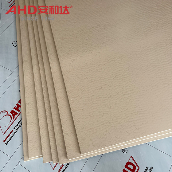
PEEK (polyetheretherketone), as a high-performance specialty engineering plastic, plays a crucial role in the semiconductor industry due to its high-temperature resistance, chemical corrosion resistance, low gas release (low exudation), high mechanical strength, good electrical insulation, and processability. Its core applications are concentrated in key components of semiconductor manufacturing equipment, precision components in clean environments, and packaging and testing processes. The following details its applications in specific process stages:
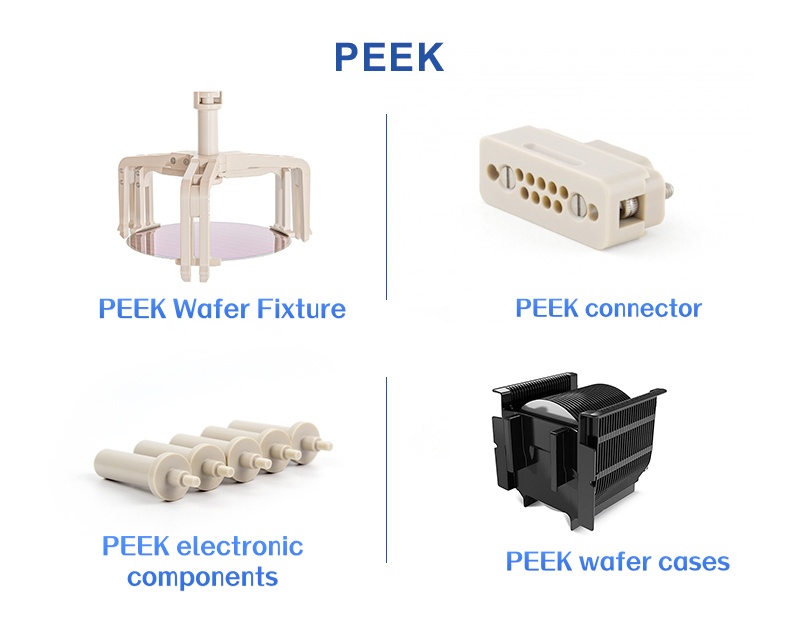
PEEK Machined Parts
Ⅰ. Core Applications in Semiconductor Manufacturing
Equipment for Semiconductor manufacturing involves multiple precision processes, such as photolithography, etching, thin-film deposition, chemical-mechanical polishing (CMP), and cleaning. Equipment must operate in highly corrosive, high-cleanliness, high-temperature/low-temperature, or vacuum environments. PEEK's comprehensive performance makes it suitable for these demanding conditions.
1. Wafer Handling and Transport Components
Wafer Carrier/Cassette: Used for wafer storage and transport, it must withstand corrosion from cleaning solutions (such as sulfuric acid and hydrogen peroxide mixtures) and plasma environments. PEEK's low gas release properties prevent contamination of the wafer surface, and its rigidity is superior to ordinary plastics, ensuring wafer flatness.
Robot End-effector: In semiconductor automated production lines, robotic arms need to precisely grip wafers. PEEK's low coefficient of friction, wear resistance, and dimensional stability reduce the risk of wafer scratches; in some applications, carbon fiber reinforcement (CF/PEEK) is used to enhance rigidity.
2. Chemical Mechanical Polishing (CMP) Equipment
CMP is a key process for wafer planarization, requiring the use of strong acid/base polishing slurries containing nano-abrasives (such as SiO₂ abrasives + ammonia/hydrogen peroxide). PEEK is commonly used in:
Retaining Rings: Used to secure the polishing pad and prevent wafer misalignment. They must be resistant to polishing fluid corrosion and abrasion. PEEK's long-term temperature resistance (250℃) allows it to withstand localized heat generation during the polishing process.
Dresser Components: Used to dress the surface of the polishing pad. PEEK's chemical resistance protects against the corrosive effects of polishing fluids.
3. Wet Etching and Cleaning Equipment
In wet etching processes, wafers need to be immersed in highly corrosive solutions (such as HF, HNO₃, KOH). Equipment components (pipes, valves, pumps, nozzles) must be chemically resistant and have low leaching. The advantages of PEEK over traditional metals or fluoroplastics (such as PTFE) are:
Higher mechanical strength than PTFE (tensile strength approximately 90-100 MPa vs. PTFE's 20-30 MPa), less prone to deformation;
Better high-pressure resistance (can withstand pressures of several megapascals), suitable for high-pressure flushing systems;
Smooth surface (coefficient of friction 0.1-0.3), reducing particle adsorption and improving cleanliness.
4. Vacuum and Plasma Environment Components
In semiconductor vacuum chambers (such as PVD and CVD equipment), materials must have low outgassing to avoid contaminating the vacuum environment. PEEK's total gas release rate (TML) is typically <1%, far lower than that of ordinary plastics, making it suitable for:
Vacuum chamber viewing window frames: replacing metal to reduce weight while avoiding metal ion contamination; Electrostatic chuck (ESC) edge stops: securing wafers and isolating them from plasma; PEEK's resistance to plasma bombardment (radiation resistance) is superior to most polymers;
Sensor housings: protecting pressure/temperature sensors in vacuum environments; low gas release characteristics ensure measurement accuracy.

PEEK Parts
Ⅱ. Sealing and Connection Components
Seals (O-rings, gaskets) and connectors in semiconductor equipment must simultaneously meet requirements for chemical resistance, high temperature resistance, and low exudation:
Seals: PEEK can be combined with perfluoroelastomer (FFKM) rubber or used directly as static seals (such as flange gaskets), replacing traditional rubber (which is prone to swelling and aging) in highly corrosive liquids or high-temperature (above 200°C) environments.
Electrical Connectors: PEEK's high insulation (volume resistivity > 10¹⁶ Ω·cm) and arc resistance make it suitable for connectors used in high-frequency signal transmission (such as RF test interfaces) to prevent signal attenuation.
Ⅲ. Packaging and Testing Stages
Semiconductor packaging (e.g., chip mounting, bonding) and testing (e.g., probe cards) require materials that can withstand high soldering temperatures (above 260°C) and have low contamination:
Test Sockets: Used for chip functional testing. PEEK's thermal stability (long-term use 250°C, short-term 300°C) allows it to withstand repeated insertions and removals and high-temperature aging. Adding conductive fillers (e.g., carbon fiber/graphite) provides electrostatic discharge (ESD) protection, preventing electrostatic breakdown of the chip.
Lead Frame Auxiliaries: In some advanced packages (e.g., fan-out), PEEK can be used as a fixture to temporarily hold the chip. Its low gas release characteristics prevent adhesive contamination.
Ⅳ.Summary
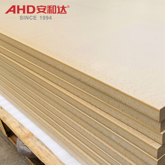
PEEK Plastic Sheet core advantages align with semiconductor demands.
The semiconductor industry has extremely high requirements for material cleanliness (low precipitation), chemical resistance (corrosion resistance), and reliability (long lifespan). PEEK becomes a key choice due to the following characteristics:
Low gas release: Prevents wafer contamination and improves yield;
Wide temperature range adaptability: Maintains stable performance from -50℃ to 300℃;
Chemical resistance: Resistant to strong acids, strong alkalis, organic solvents, and plasma;
Precision machinability: Can be injection molded and machined into complex structures (such as microchannels).
As semiconductor process nodes shrink, the requirements for material cleanliness and precision further increase. PEEK and its modified products will replace traditional metals or plastics in more high-end equipment, becoming a key basic material in semiconductor manufacturing.
Ⅴ. Core Characteristics of PEEK
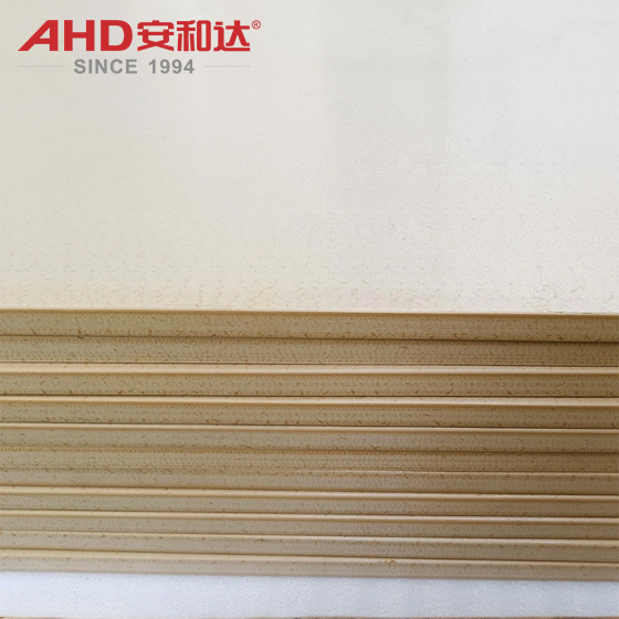
The "high performance" of PEEK stems from the synergistic effect of its molecular structure and crystallinity. The following are its key advantages that distinguish it from ordinary plastics:
1. Outstanding High-Temperature Resistance
Long-term operating temperature: -50℃ to 250℃ (continuous use); short-term tolerance to 300℃.
Glass transition temperature (Tg): Approximately 143℃ (unreinforced); Melting point (Tm): Approximately 343℃ (its semi-crystalline nature allows it to maintain a certain strength near the melting point).
High-Temperature Performance Stability: Even after long-term use at 250℃, mechanical properties (such as strength and modulus) show minimal degradation, far exceeding that of ordinary engineering plastics.
2. Excellent Mechanical Properties
High Strength and High Rigidity: Pure PEEK has a tensile strength of approximately 90~100 MPa and an elastic modulus of 3.6 GPa.
Fatigue Resistance: It is not easily broken under cyclic loading; its fatigue life is several times that of metals.
Abrasion Resistance: Excellent self-lubricating properties (coefficient of friction 0.1~0.3), with extremely low wear rate when rubbing against metal.
3. Strong Chemical Corrosion Resistance
Resistant to most organic solvents (e.g., alcohols, hydrocarbons, ketones), weak acids/bases (e.g., hydrochloric acid, dilute sulfuric acid solutions);
Soluble only in strong oxidizing acids such as concentrated sulfuric acid and concentrated nitric acid (requires high temperature and pressure conditions);
Excellent hydrolysis resistance (superior to polyester plastics such as PET), stable performance in high temperature and high humidity environments (e.g., 150℃ steam).
4. Biocompatibility and Safety
Meets ISO 10993 biosafety standards, with no cytotoxicity, sensitization, or genotoxicity;
Elastic modulus (3.6 GPa) is close to that of human bone (3~20 GPa), reducing the likelihood of "stress shielding" (bone degeneration caused by excessively high modulus in metal implants) after implantation;
Withstands high temperature and high pressure sterilization, suitable for reusable surgical instruments.
5. Flame Retardancy
Achieves UL94 V-0 rating without the addition of flame retardants; produces extremely low smoke during combustion (low smoke, non-toxic), suitable for rail transportation and aircraft interiors.
Radiation Resistance: Withstands 10⁹ Gy or higher of gamma rays or X-rays (ordinary plastics become brittle at 10⁶ Gy), suitable for use in nuclear industry equipment or medical radiotherapy devices.
6. Good Processing Performance
Can be injection molded, extruded, and machined, suitable for manufacturing complex-shaped parts (such as integrated medical devices and precision mechanical parts); Wide processing temperature range (360~400℃), but prolonged high temperatures should be avoided to prevent thermal oxidative degradation (inert gas protection or rapid cooling is required).
AHD PEEK Polyetheretherketone Sheet